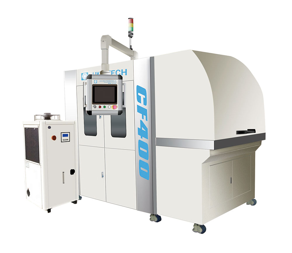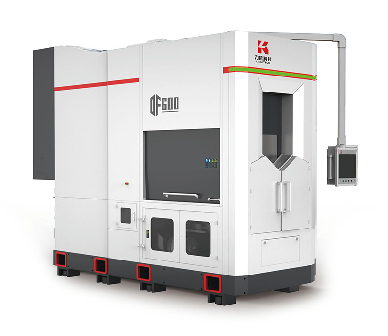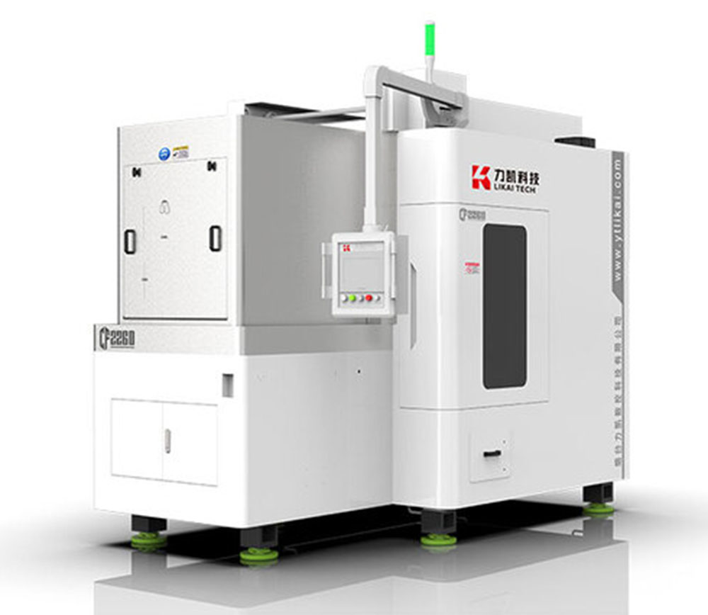


Advantage:
● High economic efficiency, hundreds and thousands wafers can be cut at a time;
● Can cut silicon ingots up to □230mm×L900mm;
● Small depth of crystal defects;
● Few geometric defects (TTV, bowing, deviation, etc.)
● Sawing thinner wafers;
● Reducing the cost of solar cells;
● CE Conformity.

Lydia Chen
Tel: +86-1314104906
Mail: lkhw@ytlikai.com
No. 7, Taipei South Road, Guxian Street,Eco-Tech Development Zone, Yantai City, Shandong Province, China
Get in Touch
By clicking 'Allow All', you agree to the storage of cookies on your device to enhance site navigation, analyze site usage and assist with our marketing efforts.
Custom Settings
Reject All
Agree All


